
GaN based Solid State Power Amplifiers have extremely attractive properties (e.g., small form factor, high efficiency, high linearity wide bandwidth, and radiation hardness that make them ideal for use on ground applications as well as for space-based satellite communication systems.
Advantech Wireless has pioneered the design and manufacturing of GaN SSPAs, with the launch in early 2010 of a full product line, covering S-, C-, X-, and Ku- satellite bands. However, limited reliability data information is available on this new technology.
The purpose of this article is to describe the underlying complexities associated with the task and to present the calculus methodology, as well as the findings of an extensive R&D program developed at Advantech Wireless in the years prior to the product launch. The theoretical results correlate with the field data and underline a major improvement in reliability, superior to all existing technologies.
For the last 70 years, the basis for various reliability and availability based decisions has been the Mean Time Between Failures (MTBF). Widely used by the telecom industry, the MTBF calculus has been associated with a large number of methods and procedures. These calculus techniques are based on different failure definition criteria and can lead to a wide range of conflicting results and misconceptions. A common error is to consider MTBF as the “Service Life,“ in other words, the expected operating time in hours until failure. In many cases, Reliability, Availability, Failure Rate and MTBF are used interchangeably, which adds to the confusion.
For the purpose of this article, Reliability is the ability of a system to perform as specified, under stated conditions, for a specified period of time, without failures. An SSPA mounted on the board of a satellite will have Reliability as a clear figure of merit, as repairs are not possible
The relation between Reliability and MTBF is as indicated below:
Availability, in this context, is the degree to which the system is operational, and accessible when required for use. It is defined by the system reliability as well as the repair or recovery time when a failure occurs.

Many telecom systems have at least 10 years of expected life, but during this time they will certainly experience failures. The figure of merit in this case is how short the recovery time is. This will apply to most ground based satellite transmission systems, where time off the air is strictly related to loss of revenue.
The Availability formula is therefore a function of MTBF and MTTR (Mean Time To Repair), and it is presented below
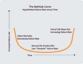
Both equations above are based on the assumption that the components suffer constant failure rates during their operating lifetime. The figure below illustrates this concept.
The normal life, is the constant failure rate life, and it is the time when the system should operate in the field. This is where the quality issues related to manufacturing, design margins, operating factors, have leveled off, and the failures are constant. The initial high failure rate area, also called Infant Mortality, should be corrected by ample factory burn-in time.
The final stage, or the Wear-Out time, should be handled by proper proactive maintenance and spare part replacement programs.
For all new developments, in the absence of field data, the only way to predict MTBF is by mathematical statistical calculus.
There are many methods suggested, but the main ones used in the telecom industry are below:
Telcordia, Previously Known As Bellcore
Offers calculation techniques for Telecom equipment, based on Mil-HDBK-217 standard, but with changes and updates to reflect measured field performance in the industry, as well as components improvements. The methodology is focused around Part Count Prediction, by assigning different failure rates to each electronic part, and on Part Stress Analysis, by assigning failure rates based on specific stress criteria (temperature, for example).
MIL-HDBK-217
Used by the U.S. Military since 1965, but now considered to be obsolete. The reason is that the methodology is based on component data reliability only, which has greatly improved since the technology’s inception. Today’s reliability investigation will show that most of the failures were caused by process control, design, or misuse in the field. The component reliability database has not been updated, as is the case with Telcordia.
Highly Accelerated Life Testing (HALT).
This method, combined with Telcordia predictions, has been widely used by Advantech Wireless on the new GaN-based family of SSPAs. This is a method used to increase the reliability of a product design by establishing how long it will take to reach the breakpoint of a product while exposed to a carefully controlled stress environment. That can include extreme high and low temperature cycling, high temperature and high voltage burn-in shock and vibration.
Figure 1. (Left) 50W Ku-band GaAs based SSPA (2006 generation), versus (Right) 50W Ku-band GaN SSPA (2010 generation)
2. GaN R&D Reliability Program
When Advantech Wireless Inc. embarked in the early 2000’s on an ambitious R&D development program of GaN based Solid State Power Amplifiers, little was known about reliability or failure modes of GaN components. The technology had been available since 1990 and was mostly used for military developments and research. The price per component was extremely high, but the technological potential was quite appealing.
In order to successfully deploy the new GaN generation of SSPAs, with an expected MTBF of minimum 10 years, concentrated research was dedicated to understanding the optimum operating points, the thermal behavior, linearity performance, efficiency, and the failure mechanisms. The prediction criteria was based on the Telcordia methodology (which is considered to be the most up to date), and on the HALT accelerated failure process. The MIL-HDBK-217 standard was avoided, as it was considered outdated.
Several electronic components and parts were ordered from various suppliers and compared in the lab. An extensive burn-in program, of over 1 Mil cumulated hours, was put in place in order to study component stability and failure modes, as per the HALT methodology. The accelerated failure program covered:
- High Speed Ambient Temperature cycling between -50 deg C to + 60 degC
- The purpose was to understand the device behavior under extreme temperature cycling, accelerate failures due to improper assembly techniques, determine the optimum heat transfer mechanism
- Burn-in at junction temperatures between +150 deg C to + 200 deg C
- The purpose was to allow fast aging and early failure mechanisms due to high operating temperature points as defined by Telcore and HALT, as well as provide feedback to design engineers on aspects related to mechanical package and cooling system design
- Burn-in at high junction temperature and variable drain/gate voltages, no RF input
- The devices were set in burn-in with drain voltages between+20 VDC to+ 60 VDC, and gate voltages from -0.5 VDC to- 5 VDC. Junction temperature was set up to 250 deg C, and no RF input was applied.
- Burn-in at high junction temperature and variable drain/gate voltages, with RF input
- The devices were set in burn-in with drain voltages between +20 VDC to +60 VDC, and gate voltages from -0.5 VDC to- 5 VDC. Junction temperature was set up to 250 deg C, and the devices were driven in saturation with RF input.
- Shock and vibration.
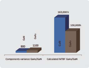
Figure 2. 100 W Ku-band component and MTBF variance GaAs (Gray) versus GaN (Blue)
Power Amplifier assemblies were exposed to random vibration cycles, up to 20G high. The purpose was to define long term mechanical integrity of the devices, considering the intrinsic crystal structure.
The HALT accelerated breaking program highlighted failure mechanisms that were also reported in similar research studies including the European Space Agency, NASA (Air Force Research Laboratory), and IEEE publications.
At the start of this six year R&D program, the failure modes could be grouped in:
- Current Collapse, which manifests as drain current decreases under specific temperature, drain voltage, RF drive levels. This phenomena could be reversible, as a function of drain voltage, or irreversible, when permanent damage occurred. The cause was studied in the scientific community and was associated to ‘Electron Trapping’ in the dielectric interface. Due to the high energy levels (high RF fields and high Drain Voltage), high energy electrons would get trapped into the dielectric, causing drain current decrease.
- Gate Leakage degradation mechanisms. Under High Drain Voltage bias, and high RF drive levels, the peak voltage on the drain can get very high. That high voltage will cause quantum mechanical electron tunneling. The electric field at the gate edge will increase enough to cause current leakage, or electron trapping. This translates into a degradation of in DC current, low output RF power. This phenomena was not noticed on devices exposed only to burn-in/ No RF drive.
- Inverse Piezoelectric Effects. High voltage bias on the gate edge under drain bias can generate inverse piezoelectric effects. These high electric fields can generate strain in the crystal structure of the GaN device. When a critical gate-drain voltage is reached, defects could develop in the crystal, which will lead to electron trapping and gate leakage current.
The main failure modes were analyzed and results compared with suppliers design targets and factory test results. Feedback was provided and a new set of design rules and improvement requests was put into place with a selected group of component manufacturers.
A new generation of GaN based components was manufactured and considerable improvement was achieved. By improving manufacturing processes, by use of special gate and drain layer materials, surface passivation, and others, meantime to failures values have reached by year 2010 incredible values of over 1 Million hours at 200 deg C junction temperature. These values show the remarkable increase compared to any other existing solid state technology.
As an example, GaAs based transistors will be permanently damaged at 175deg C junction temperature.
These major improvements in GaN component technology were also matched by a new generation of optimization and linearization circuitry, developed by Advantech Wireless, and introduced in all GaN based SSPAs manufactured since the initial product launch in early 2010.
Safe bias operating points were defined as per calculated temperature profiles. These allowed strict control of earlier reported current collapse, and gate leakage / inverse piezoelectric effects.
The Telcordia prediction calculations provided initial calculated MTBF numbers.
For this analysis, a 100 W Ku-band GaAs based SSPA, built by Advantech Wireless prior to 2011, was compared with a 100 W Ku-band built using recent GaN technology. The focus was concentrated on these critical areas:
– RF Power module
– Power supply module
– Process control
These two modules of any SSPA (or TWT design) would be the ones generating 90 percent of the field failures. Any major reliability improve program, will therefore need to focus on improving these two building blocks.
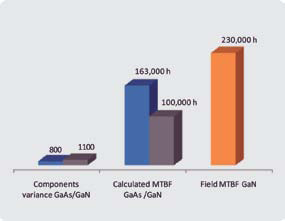
Figure 3. 100W Ku-band GaAs versus GaN, MTBF, field MTBF
3. RF Power Module Reliability
The immediate argument comes from the fact that GaN transistors can handle close to 10 times higher power density per surface area as opposed to GaAs or other devices. That means higher power transistors can be built, while using less of them to achieve the 100w of Ku-band power.
The Telcordia prediction method is counting similar components (for example high power Ku-band transistors, capacitors, and so on) and assigns them to various groups. Each group has its own quality factor and a generic failure rate. The group failure rate is calculated by multiplying the number of components with the specific failure rate. The total failure rate is calculated by adding all group failure rates. All equations are based on field experiences of telecom equipment.
It is in this context obvious that by using less components, Reliability and MTBF will increase.
It has been noted that the 100W Ku-band GaAs SSPA was using approximately 30 percent more active electronic components then the equivalent 100W Ku-band GaN based SSPA. Based on Telcordia calculations, we would expect from the beginning a similar 30 percent improvement over MTBF.
Telcordia also takes into account each component failure rate as function specific stress levels, in this case temperature. If the components are designed to handle higher temperature, the reliability is higher. As a rule of thumb, for each 10 deg C of increase in temperature, MTBF will decrease by 30 percent.
If GaN devices can handle now up to 25 deg C higher temperature with no degradation in performance, it is expected the final RF Power Amplifier MTBF to increase by at least 60 percent.
4. Power Supply Module
One major benefit of using GaN transistors in SSPA design is the fact they operate at higher voltages.
This has immediate impact on the power supply design. If, for example, we need to bias the 100W Ku-band GaAs SSPA at +12 VDC, we need to design a power supply able to generate 120 Amps. This is by no mean a trivial task, considering the small real estate available, the component ratings, and the limited cooling capabilities.
By comparison, the same power supply, when designed for GaN based SSPAs, will need to operate at +48 VDC, and , therefore, generate only 30 Amps. This will greatly benefit the power supply design and will have a major improvement in reliability.
The second major benefit of using GaN transistors, is the fact that they are much more efficient. As an example, a 100W Ku-band GaAs based SSPA, will consume at least 30 percent more energy than the equivalent GaN based design.
Higher efficiency, combined with low operating bias current, provide a major improvement in the overall reliability of the power supply module in GaN based SSPAs. (See Figure 2 on the next page.)
5. Process Control
Unfortunately, none of the reliability calculation standards take into account the manufacturing processes. All of them are based on component reliability.
This is why MIL-HDBK 217 so quickly became obsolete. The components reliability numbers that the standard was using had not been updated since 1965. Over the last 49 years, the reliability figures for the electronic components have largely improved. A look into today’s failure mechanisms reveal that the most likely ones are caused by product design, process control, or human errors.
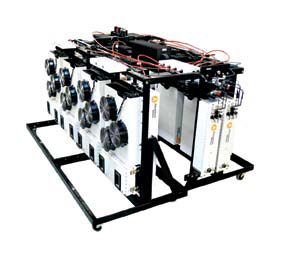
Advantech Wireless’ 3kW Ku-band system GaN-Based SapphireBlu Series
This is why we believe the process control is a most important part of the design activities and any Reliability Improvement Program.
If we are looking just at the components alone, two companies building the same product, per the same bill of materials, should both have identical MTBF. This is not the case most of the time.
We have all witnessed, so many times, great products with perfect reliability and quality falling apart when production is relocated. What is changing in most of these cases are the manufacturing processes, while the bill of materials remains the same.
At Advantech Wireless, process control is part of all design objectives. Identifying the design limits and risks requires extensive product aging through combinations of stress factors. This is always required in order to move the product life out of infant mortality range.
For the GaN product line, several key process controls can be identified below:
– 96 hours burn-in on all active devices at specific high temperature and voltage settings
– 96 hours burn-in on power supply at specific high temperature and current ratings
– 24 hours temperature cycling on all printed circuit boards
– Unique proprietary techniques in assembling the GaN components, which allows much better heat dissipation.
– 24 hours environmental testing of the final product, in thermal chamber, from extreme cold to high temperature
– 96 hours additional active burn-in for final product at high temperature
These severe (and expensive) aging and screening processes provide an overall remarkable increase in real-life, field measured, MTBF.
For the purpose of this calculus, a population of 500 units deployed in the field were analyzed over the last four years.
A 3.8 percent failure rate per year was identified and recorded.
Considering the MTBF as the inverse of the failure rate, the field MTBF number for this sample population was:
Field MTBF= 1/0.038 = 26.3 years= 230,388 hours
Conclusion
By controlling all failure mechanisms, by working closely with strategic GaN components manufacturers, and by achieving deep levels of understanding of GaN internal physics, Advantech Wireless engineers have developed a new generation of SSPAs with unmatched electrical performance and high reliability.
Statistical reliability calculation based on existing standards have shown for the GaN-based SSPA a remarkable 65 percent increase in MTBF as compared to the similar GaAs based SSPA product. These calculations are in line with expectations, based on components reliability, number of components used, and electrical efficiency.
When combined with strictly controlled manufacturing processes, tailored on the specific failure mechanisms identified on GaN devices, the field MTBF is even higher, exceeding an impressive 130 percent improvement over the equivalent GaAs based product. With the new SapphireBlu™ Series of high power SSPAs now able to reach up to 6 KW in RF power, the Advantech Wireless line of GaN based SSPAs is well positioned to meet the most stringent environmental and the most demanding work conditions.
To learn more about Advantech Wireless, please go to http://www.advantechwireless.com/

About the author
Cristi Damian is the Vice President, Business Development, at Advantech Wireless. He joined Advantech Wireless in 1995 where he held various leading positions in Operations, Manufacturing, Sales, Engineering and Customer Support. Prior to Advantech Wireless, he acquired experience as a hardware engineer in various high-tech companies. Mr. Damian holds a Master’s degree in Electrical Engineering from Concordia University.