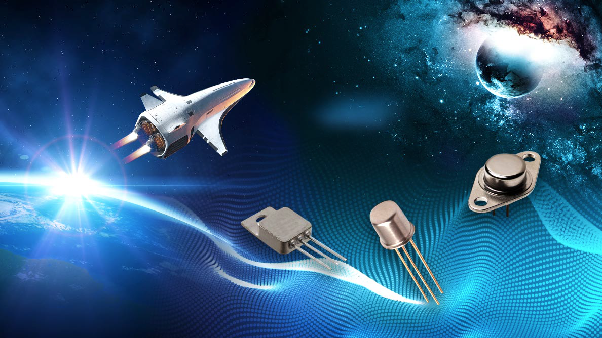
New Space designers are renewing their interest in traditional metal case devices. While hermetic devices have been popular design choices over the last few decades, the appeal of compliance and reliability has designers revisiting the Transistor Outline (TO) JEDEC packages that were once the go-to option for space electronics.

There was a time when designers of small signal componentry turned to TO-18 and TO-5 devices, as well as TO-66 and TO-3 packages which are considered ideal for high-voltage and high-power applications. Industry evolution and design challenges drove engineers to embrace more modern metal case hermetic packages such as TO-257, TO-254, and TO-258. While these were easier to deploy than their more traditional case counterparts, over the last two decades, even they were ultimately displaced by their surface mount equivalents.
UA and UB packages are often deployed for small signal use, while SMD-05 and SMD-1 are recognized for applications demanding increased power. Today, the need for proven compliance and reliability is driving a return to the TO metal cases of earlier design days.

TO Technology Takes New Space Back To The Future
Commercial missions and New Space design have pushed circuit board design from using ceramics to the use of FR4 board materials. The attachment of large-scale surface mount parts can be cause for concern; it is now a caution in ESA’s Space Product Assurance Classification ECSS-Q-ST-70-38C that component suppliers must ensure CTE compliance when these designs are employed within Class 1 boards, such as glass fiber epoxy or glass fiber polyimide resins.
While lower mass advantage can be achieved with UA and UB packages, soldering of the devices is a technically challenging process that adds design risk. Packages with larger mass and surface areas are also vulnerable to failures, for example SMD-05 and SMD-1 based designs.
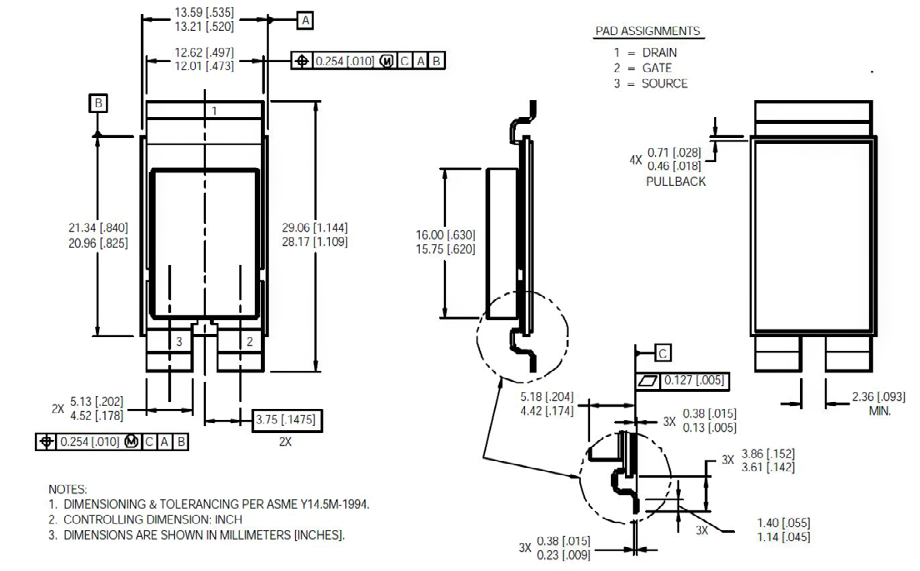
Joint areas are particularly susceptible to stress fractures, increasing the risk of catastrophic mission failure. Cracking can also occur in SMD packages mounted above a large ground plane and exposed to the extensive thermal cycles common in space electronics. Figure 1 on the following article page demonstrates a potential solution to this problem, a CTE compliant mounted package or carrier featuring dual lead connections.
Traditional leaded packages also require engineering expertise, due to stray inductances that can introduced via additional lead length over surface mount packages. This can affect switching performance and must be mitigated by expert circuit layout, designed to prevent oscillation within the circuit.
 Click to enlarge.
In contrast, metal case transistors are proven to offer some degree of compliance, with the leads acting as an expansion route during thermal shocks. Metal case transistors are generally better at dissipating system heat, especially valuable as switching applications become faster, chips become smaller, and both reach their respective control limitations. Extra care is required when a gold flash is present on the lead termination. Gold contamination within a PCB soldering connection can make the joint more brittle, making it essential to remove the gold flash and its associated risk prior to assembly.
When commercial off the shelf components are used, they are typically solder dipped with RoHS compliant sac type solders. However, lead finished solders are more reliable in mission critical setting and are often approved under the RoHS regulation by exception for military, avionic and space applications.
Similar reliability concerns are why tin-plated terminations on plastic devices are often not used, a caution against the known risk of tin whiskers which can quickly short out transistors.
When producing a PCB for space electronics, it is imperative that RoHS compliant and non-RoHS compliant solder assemblies, for example wave soldering or reflow systems, are manufactured separately to prevent cross-contamination of sac and leaded solder.
Upgradable value TO solutions offer options to optimize configurations, including the ability to mix technologies or manufacturers’ die within the package. TO packages can also mitigate the risk of poor soldering of surface mount packages onto PCBs where visual inspection is not easily managed.
In this innovative fourth age of space, successful designs may demand either or both metal case leaded devices or surface mount technologies. Both may support the mission, and both must be tested in accordance to Mil standards or ESA specifications using screening options such as NS1 and NS2.
The NS1 sequence includes traceability to all materials and operations, and provides an assurance foundation for manufacture using robust, controlled, space-proven processes and designs. NS2 provides next level assurance by adding baseline mechanical and electrical screening.
Metal transistors offer a simplified path to upgrade, in contrast to surface mount options. For example, footprints are identical between the plastic TO-220 package and the TO-257. Prototyping can be managed using low cost components, proofing a design that can easily be transferred to more robust packaging optimized for harsher environments.

This advantage has great impact in New Space design, as cost effectiveness of components is a key growth driver of higher volume satellite constellations in Low Earth Orbit (LEO). Heritage technology clearly has continued influence on New Space design, providing compliance and reliability that has long-term engineering value.
www.ttelectronics.com
With more than 30 years’ experience in the semiconductor and space industries respectively, Rob is one of the founders of TT’s New Space Electronics® and is the company’s technical expert in this field. Connect with Rob at robert.coleman@ttelectronics.com or via LinkedIn.

